
2026 Global Semiconductor Report: Advanced Packaging, Full Industry Chain, and Expansion Opportunities
The semiconductor industry is currently in a dual dividend period driven by “AI computing power + accelerated domestic substitution,” where advanced packaging, as the core path to performance breakthroughs in the post-Moore era, is driving the comprehensive expansion of the entire industry chain from equipment to materials.

The complete report data charts and the end-of-article reference report collection (PDF) have been shared in the members group
This report draws insights from the 102 global semiconductor industry research reports and datasets listed at the end, including the “World Semiconductor Trade Statistics: 2026 Global Semiconductor Market Forecast Report” and “Bernstein: 2026 Global Semiconductor Report: Stacking Higher, Selling Higher,” systematically examining the growth logic of four core tracks—advanced packaging, HBM, CoWoS, and CBA. From 2025 to 2030, stacked-wafer usage is set to grow sevenfold, the memory chip market will surpass $1 trillion within three years, and the localization rate of domestic equipment will climb from 1% toward 30%. The complete report data charts and the latest reference report collection at the end have been shared in our exchange group—read the original text, join the group for consultation, and customize data and reports to grow alongside 800+ industry professionals. Whether you are a semiconductor equipment manufacturer seeking high-growth niches or an industry investor evaluating long-term positioning, this report clarifies the “technology iteration → capacity expansion → domestic substitution” industry chain, helping you seize the certain opportunities within the trillion-scale market.
I. Core Industry Conclusions (Opening: Anchoring the Dividends Catalyzed by Computing Power)
The expansion of AI computing power resonates with the slowing of Moore’s Law, and the global semiconductor industry is entering a golden cycle of “stacking-driven growth.” Data shows that global stacked-wafer usage will climb from 500k wafers/month in 2025 to 3,500k wafers/month in 2030, with a five-year CAGR exceeding 45%. Among these, the three segments of HBM, CoWoS, and NAND-CBA contribute over 70% of the incremental growth, directly driving synchronized demand explosions in supporting segments such as equipment, substrates, and bonding consumables, echoing the World Semiconductor Trade Statistics’ forecast that “the global semiconductor market will surpass $1.5 trillion in 2026.”
Semiconductor Industry Global Equipment Market Size Line Chart 1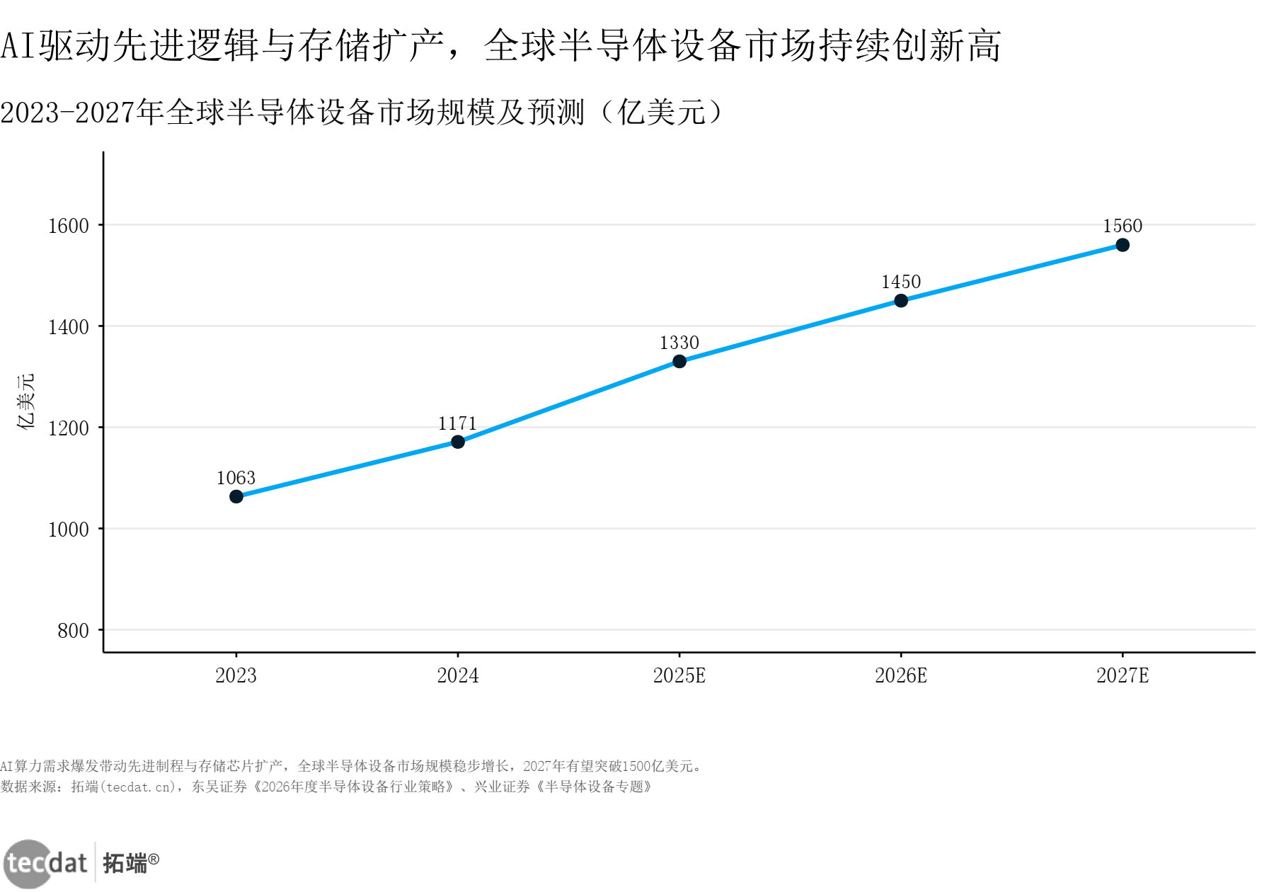
Chart interpretation: From 2023 to 2027, the global semiconductor equipment market size continues to rise. Driven by the dual engines of AI advanced-process R&D and memory capacity expansion, the industry scale will grow from $106.3 billion to $156 billion, with an average annual CAGR exceeding 10%. As the “leading indicator of fab capacity expansion,” the equipment segment is the first to benefit within the industry chain, highly aligned with the overall global semiconductor growth trend. Action for relevant audiences: Equipment distributors should prioritize the distribution of etchers, cleaners, and other equipment whose localization rate has exceeded 50%, reducing market education costs; small and medium equipment component manufacturers can focus on R&D of precision fixtures and bonding consumables for HBM, entering high-value-added niches and capturing fab expansion orders.
One-sentence investment thesis: Continuously rising computing power demand accelerates fab expansion, and the equipment segment benefits first due to its “invest first, produce later” nature; domestic substitution targets enjoy stronger certainty under policy and supply-chain security demands.
Semiconductor Industry Global Foundry Market Share Donut Chart 2
Chart interpretation: The global foundry market shows a “top-concentrated, tiered competition” pattern—TSMC monopolizes 72% of the advanced foundry share through its 3nm and 2nm advanced processes, mainly serving high-end clients such as Apple and NVIDIA; SMIC and Hua Hong Semiconductor focus on 28nm and above mature processes, relying on domestic automotive electronics and industrial control demand. By 2025, the domestic mature-process foundry capacity share had risen to 28%, and is expected to exceed 40% by 2027, becoming the core force absorbing the global mature-process transfer. This article is excerpted from Tecdat’s “2026 Global Semiconductor Industry In-Depth Report: Advanced Packaging Driving Full Industry Chain Expansion.” To access the full text, visit the Tecdat official website to search and view.
Most Popular Insights
- 2026 AI Computing Power Large Model Special Report: Computing Cloud, Edge, and Terminals, and the Landscape | With 200+ Reports and Data Collection Download
- 2026 Humanoid Robots: From Technological Breakthrough to Ecosystem Definition | With 200+ Reports and Data Collection Download
- 2026 AI Artificial Intelligence Healthcare Report: Medical Devices, Surgical Robots | With 240+ Reports and Data Download
- 2026 Humanoid Robot Dexterous Hand Industry Report: Industry Chain and Market Space | With 100+ Reports and Data Collection Download
- 2026 One-Person Company (OPC) Development Research Report: Evolution from Tool to Ecosystem | With Report PDF, Data, and Visualization Template Download
II. Full Interpretation of Policy Dividends
Global semiconductor industry policies feature “competitive support,” with domestic and overseas markets forming differentiated strategic directions, further reinforcing the long-term logic of “domestic substitution.” At the domestic level, the third phase of the Big Fund focuses on “chokepoint” segments such as advanced packaging, semiconductor equipment, and electronic chemicals, reducing corporate innovation costs through combined policies such as R&D subsidies (up to ¥50 million), tax incentives (increased super-deduction ratio for R&D expenses), and capacity subsidies. The US, Japan, and South Korea focus on competition in HBM and 3nm-and-below advanced-process capacity, attempting to consolidate market dominance through technological barriers—which instead forces the domestic industry chain to accelerate its autonomous and controllable progress, supporting the industry forecast that “domestic semiconductor equipment demand will grow 30% in 2026.” In terms of localization rates, different segments show significant divergence: the localization rates of etchers and cleaning equipment have exceeded 50%, entering the stage of scaled substitution; while the localization rates of lithography and metrology equipment are only 1% and within 10% respectively, leaving huge substitution space and long-term benefits from policy tilt and overseas supply restrictions.
Semiconductor Industry Equipment Localization Rate Scale Chart 3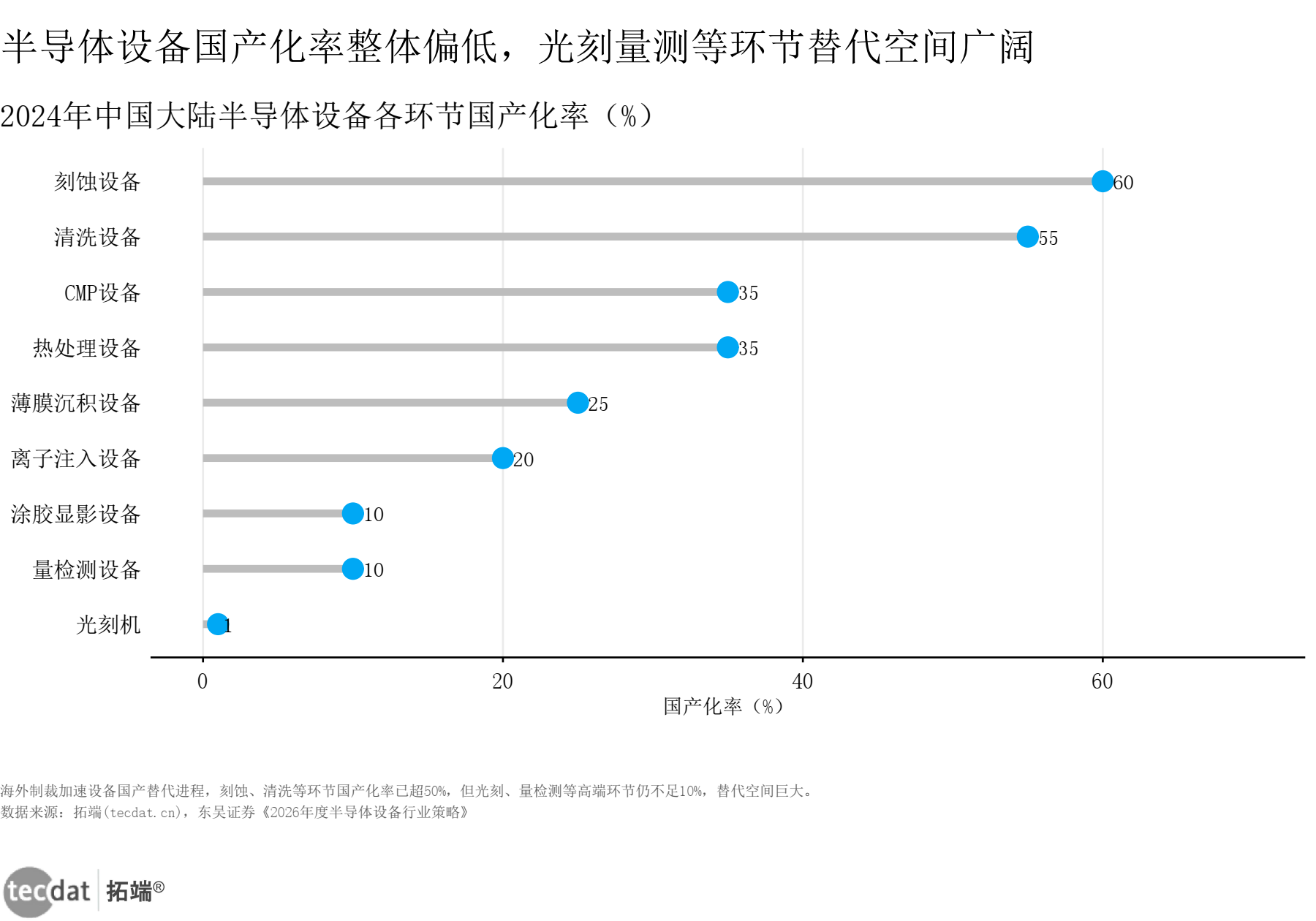
Chart interpretation: Equipment localization shows the characteristic of “mature first, high-end lagging.” Mid-to-low-end equipment such as etchers and cleaners has achieved self-supply; in 2025, domestic etcher manufacturer “AMEC” entered TSMC’s advanced-process production line validation. However, high-end equipment such as lithography and metrology remains highly dependent on imports, becoming a core weakness in industry-chain security and implying extremely high growth ceilings in related fields—the domestic lithography equipment localization rate is expected to exceed 5% by 2027. Action for relevant audiences: New materials startups should avoid the red-ocean competitive tracks of cleaning and general etching, instead entering niches such as lithography-supporting specialty photoresists and metrology calibration reagents, leveraging policy dividends to reduce R&D and market validation costs—for example, connecting with semiconductor materials special subsidies in Shanghai, Shenzhen, and other locations.
One-sentence investment thesis: Policy tilt + overseas supply restrictions create a double advantage; high-end equipment consumables, due to “domestic substitution imperatives + high technical barriers,” become the optimal direction for domestic entrepreneurship, with strong long-term growth certainty.
III. Industry Prosperity Fundamentals (Market Space TAM Estimation)
3.1 Memory Track: AI-Driven Architecture Innovation, Market Size Growing Exponentially
AI servers’ demand for high-bandwidth, low-latency memory drives memory chips from “capacity competition” to “architecture competition,” becoming the fastest-growing segment of the global semiconductor market—consistent with the World Semiconductor Trade Statistics’ forecast that “memory chip scale will exceed $800 billion in 2026.” HBM (High Bandwidth Memory), as the core supporting component of AI chips, is rapidly iterating from HBM2e to HBM3 and HBM3e. The global memory market size reached $235.4 billion in 2024 and is expected to exceed $1,000 billion by 2027, with a three-year CAGR exceeding 50%. Among these, HBM capacity will reach 758k wafers/month by 2027, while NAND achieves dual breakthroughs in capacity and performance through CBA (Cell Block Array) stacking technology. Domestic manufacturer “YMTC” has achieved mass production of CBA technology, becoming the core growth pole of the memory track.
Semiconductor Industry Global Memory Market Size Polygon Bar Chart 4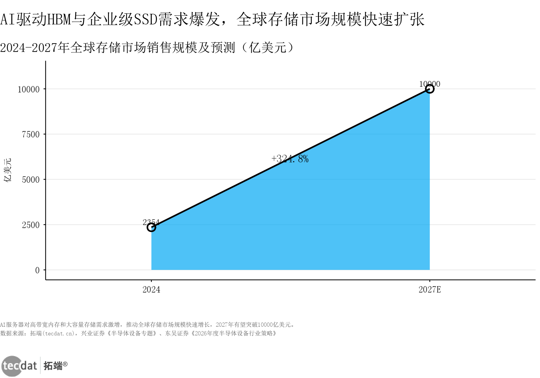
Chart interpretation: From 2024 to 2027, the global memory market size will grow by over 325%, with HBM and CBA technologies as the core drivers—HBM benefits from increased per-server usage in AI servers (from 4 to 16 units), while CBA reduces NAND unit-capacity cost through architectural innovation (30% drop in cost per GB). Together they open up memory market growth space, with domestic memory manufacturers contributing over 20% of incremental capacity. Action for relevant audiences: Memory traders should prioritize connecting with domestic NAND fabs such as YMTC and ChangXin Memory, establishing partnerships through small-batch trials (e.g., 1,000 wafers/batch) to lock in capacity ahead of time; memory module manufacturers can focus on R&D of AI-server-specific memory modules to enhance product value-added—for example, HBM3 modules suited for NVIDIA H100 chips.
One-sentence investment thesis: The HBM price-increase cycle continues (unit price expected to rise 20% in 2026) + NAND architectural innovation brings cost optimization, and the upstream and downstream memory trade and foundry segments will continue to realize dividends, while the capacity ramp-up of domestic fabs provides incremental opportunities for the local supply chain.
3.2 AIDC Power Supply Track: Computing Power Consumption Surges, Power Architecture Ushers in Innovation
The power consumption of AI computing centers is growing exponentially (single data center power consumption rising from 10MW to 50MW). Traditional power architectures can no longer meet the “efficient, stable, and miniaturized” demands, driving power products to iterate from “traditional PSU (Power Supply Unit)” to “HVDC (High Voltage Direct Current)” and “SST (Solid-State Transformer),” becoming an undervalued incremental track in the semiconductor industry chain. From 2025 to 2028, the traditional PSU share in the AIDC power market will drop from 65% to 30%, HVDC share will rise from 25% to 45%, and SST, as an emerging technology, will rapidly climb to 25%, forming a “three-tier product gradient” pattern that directly drives power semiconductor demand (5x increase in per-unit power semiconductor usage).
Semiconductor Industry AIDC Power Segment Market Percentage Stacked Area Chart 8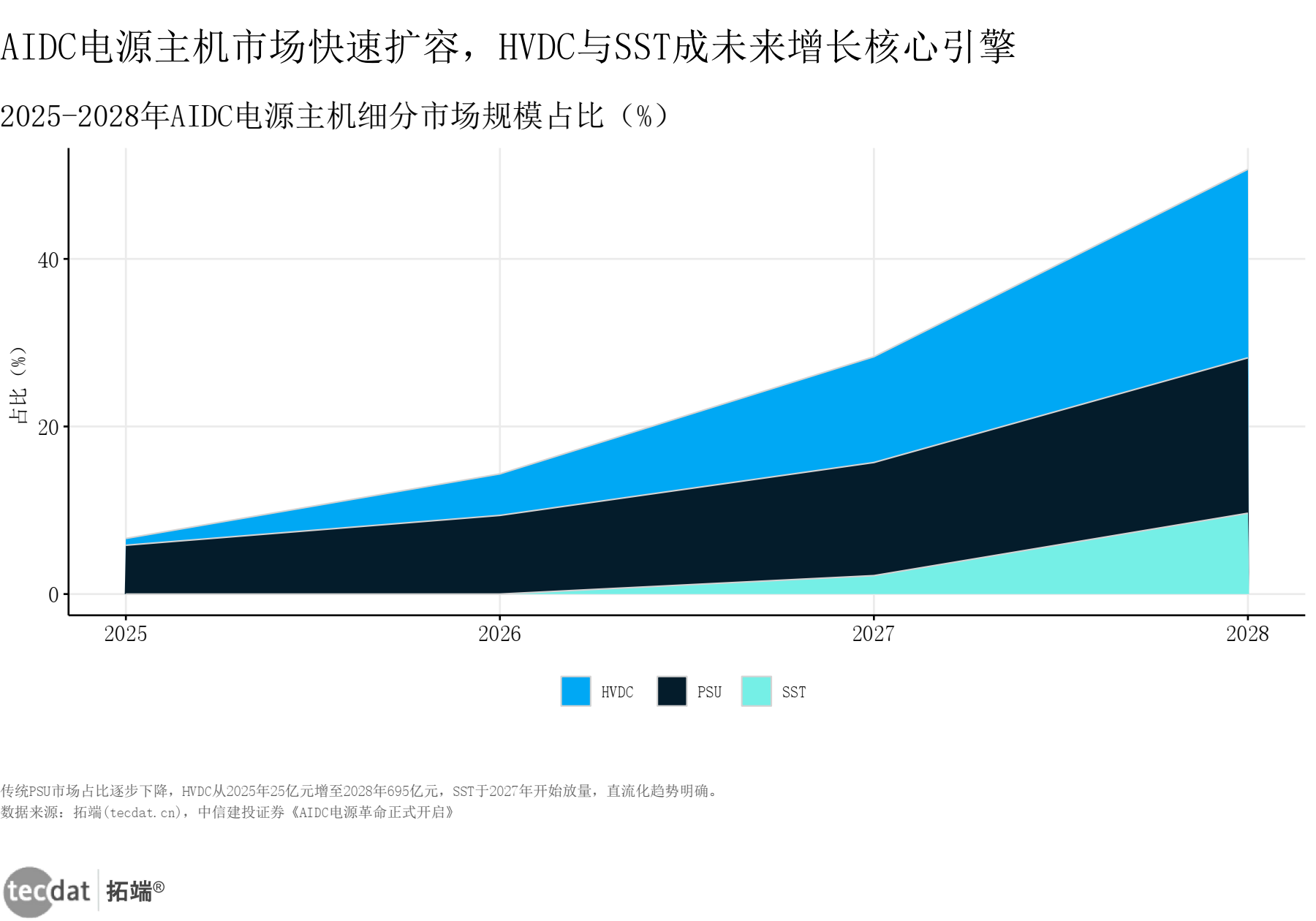
Chart interpretation: The AIDC power market is undergoing structural transformation. Traditional PSUs are gradually being replaced due to low efficiency (85% conversion) and large size, while HVDC has become the current mainstream thanks to “high efficiency and energy savings (95% conversion) + stability and reliability.” In 2026, domestic HVDC manufacturer “Huawei Digital Power” secured AI data center orders exceeding ¥1 billion; SST has begun pilot trials in hyperscale data centers, with huge future growth potential, directly driving demand for power semiconductors such as IGBT and SiC. Action for relevant audiences: Power component factories should focus on HVDC-supporting high-frequency inductors and IGBT modules, as well as wide-bandgap semiconductor materials for SST (such as SiC wafers), building up technology in advance to respond to market demand shifts—for example, connecting with domestic SiC manufacturer “SICC” for small-batch supply.
One-sentence investment thesis: AIDC infrastructure expansion drives power architecture innovation; power semiconductors show segmented increments due to “increased per-unit usage + technology upgrade,” with high-voltage and high-frequency products becoming the growth mainstay—the relevant market size is expected to exceed ¥50 billion by 2027.
IV. Industry Chain Investment Priority Map (Advanced Packaging as the Main Line)
Evaluated from three dimensions—”technical barriers + demand growth + domestic substitution space”—the semiconductor industry chain investment priority ranking is: advanced packaging supporting equipment > memory materials > power semiconductors > traditional logic foundry consumables > low-end discrete devices, consistent with the global semiconductor trend of “advanced and mature processes driving in dual wheels.”
1. First tier (high priority): Bonding equipment, grinding equipment, and test equipment (representative companies: DISCO, Advantest), benefiting from advanced packaging capacity expansion (global advanced packaging capacity grows 40% in 2026), with high technical barriers and low domestic substitution rates (below 20%), demand growth exceeding 30%; domestic manufacturer “TFME” has achieved small-batch mass production of bonding equipment;
2. Second tier (mid-high priority): HBM substrates, NAND-supporting wet chemicals, and electronic gases, benefiting from memory and advanced packaging demand, with domestic substitution rates in the 10%-30% range, possessing the dual growth logic of “demand + substitution”; domestic wet chemicals manufacturer “Anji Technology” has entered TSMC’s supply chain;
3. Third tier (mid priority): Mature-process wafers and general PCBs, with stable demand but fierce competition, domestic substitution rates already exceeding 50%, growth mainly relying on capacity expansion; domestic wafer manufacturer “NSIG” will surpass 1 million 12-inch wafers/month in capacity by 2026.
Semiconductor_Advanced Packaging Technology Evolution Infographic 3
Chart interpretation: Advanced packaging technology has gradually iterated from “wire bonding” to “2.5D/3D hybrid bonding,” with each technology upgrade driving up the value of equipment and consumables—hybrid bonding equipment unit prices are 3-5x those of traditional bonding equipment (rising from ¥5 million/unit to ¥20 million/unit), and bonding consumable unit prices more than double, making it the fastest-growing value segment in the industry chain; the global advanced packaging market size is expected to exceed $30 billion by 2026. Action for relevant audiences: Packaging foundries should prioritize CoWoS outsourcing foundry business, accumulating advanced packaging process experience through cooperation with domestic AI chip design companies (such as Cambricon and MetaX), gradually breaking TSMC’s technology monopoly—for example, undertaking test packaging orders for AI chips.
One-sentence investment thesis: Advanced packaging technology iteration brings increased value of equipment and consumables; supporting suppliers see continuous profit improvement due to the dual logic of “technical barriers + domestic substitution,” and the domestic advanced packaging supporting market size is expected to exceed ¥100 billion by 2027.
Semiconductor_PCB Semiconductor-ization Value Leap Infographic 5
Chart interpretation: AI server PCB layers and materials are comprehensively upgraded, iterating from traditional 8-layer boards to 24-layer boards; per-unit PCB value rises from ¥500 to over ¥1,500, more than doubling versus traditional products. Domestic PCB manufacturer “SCC” has achieved mass production of 24-layer AI server PCBs, with related revenue share expected to exceed 30% by 2026. Action for relevant audiences: Small and medium PCB enterprises should eliminate low-end consumer electronics board capacity (such as mobile phone PCBs) and shift to R&D of high-end substrates for foundry support, such as HBM substrates and CoWoS substrates, to meet the supporting needs of SMIC and Hua Hong—for example, developing high-density substrates suited for 3D stacking.

2026 Global and China Semiconductor Manufacturing Market Forecast and Chip Industry Analysis Report: AI-Driven, Localization, Advanced Packaging Lithography Technology | With 100+ Report PDFs, Data, and Visualization Template Download
In 2025, the global semiconductor industry stands at a critical crossroads of technological innovation and supply chain restructuring. The explosive growth of AI large models has made high-end computing chips and high-bandwidth memory (HBM) the core of demand, directly pushing the technology iteration of key segments such as lithography machines, advanced packaging, and photoresist into “high gear”; driven by both geopolitical competition and the national strategy of “scientific and technological self-reliance,” domestic substitution has shifted from “optional” to “mandatory,” becoming the core proposition for the breakthrough of China’s semiconductor industry. From wafer manufacturing to packaging and testing, from equipment materials to end applications, every segment of the industry is undergoing unprecedented transformation, with both opportunities and challenges.
Explore InsightsV. In-Depth Breakdown of Segmented Tracks
5.1 HBM & Memory CBA: Domestic Manufacturers Accelerate Breakthrough
The HBM technology route shows a pattern of “international divergence, domestic catch-up”—SK Hynix, Samsung, and Micron lead HBM3e mass production, while domestic manufacturer “ChangXin Memory” has entered the HBM2e sample delivery stage, expected to achieve mass production by 2027; NAND-CBA technology was first implemented by Kioxia and YMTC, and global NAND-CBA capacity will reach 1,057k wafers/month by 2030, with domestic capacity exceeding 30% of the total; YMTC’s CBA technology yield has improved to 85%, approaching the level of international leaders.
5.2 CoWoS & WMCM: Domestic Opportunities Under TSMC Monopoly
TSMC’s CoWoS capacity will reach 197k wafers/month by 2027, accounting for 70% of global capacity, with orders from major clients such as Apple and NVIDIA fully booked; domestic manufacturer “JCET” adopts a combined strategy of “CoWoS outsourcing + independent R&D,” breaking through 10k wafers/month of CoWoS capacity in 2026, mainly undertaking orders from domestic AI chip manufacturers; Apple’s adoption of the WM (Wafer-Level Molded) architecture drives incremental panel-level packaging, and domestic packaging manufacturer “TFME” has launched WMCM technology R&D, expected to achieve mass production by 2028.
Semiconductor Industry Top Foundry Monthly Capacity Horizontal Bar Chart 5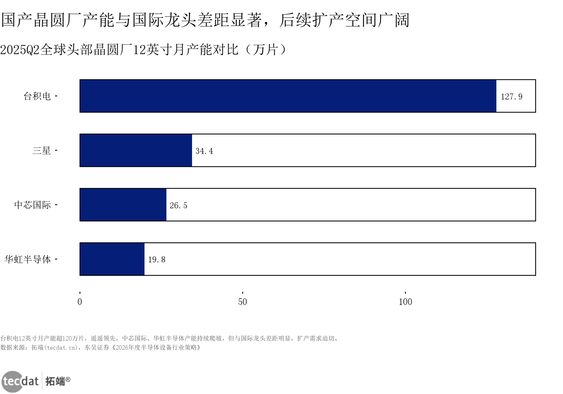
Chart interpretation: TSMC’s 12-inch monthly capacity (1.5 million wafers/month) far exceeds domestic manufacturers (SMIC 350k wafers/month, Hua Hong Semiconductor 200k wafers/month), but local fabs have ample expansion space—SMIC’s new Shanghai plant will add 200k wafers/month by 2027, and Hua Hong Semiconductor’s Wuxi plant will add 150k wafers/month, mainly focusing on 28nm and above mature processes to absorb global capacity transfer demand. Action for relevant audiences: Local equipment manufacturers should focus on mature-process transformation and upgrades—for example, developing etchers and thin-film deposition equipment suited for 28nm processes, connecting with SMIC’s and Hua Hong’s expansion orders, avoiding direct competition with international leaders in advanced-process equipment.
One-sentence investment thesis: Leading giants continue to expand capacity; domestic equipment, thanks to “mature-process适配 + cost advantage,” sees an extended validation window, and the domestic mature-process equipment localization rate is expected to exceed 60% by 2027.
5.3 CPO Optical Interconnect Segment: Low-Power Demand Drives Technological Innovation
AI data centers’ demand for low power consumption (per-cabinet power dropping from 50kW to 30kW) drives optical interconnect technology to iterate from “traditional pluggable optical modules” to “CPO (Co-Packaged Optics).” CPO reduces power consumption by 70% compared to traditional optical modules (from 10W/port to 3W/port). The global CPO market size is expected to exceed $5 billion by 2026, and domestic manufacturer “Innolight” has achieved CPO sample delivery, expected to enter mass production by 2027.
Semiconductor Industry Optical Module Power Comparison Semicircle Donut Chart 10
Chart interpretation: CPO technology has significant advantages in power consumption. Traditional pluggable optical modules (100G) consume about 8W/port, while CPO (400G) consumes only 3W/port, suited for AI data centers’ “power reduction” needs. In 2026, cloud vendors such as Meta and Microsoft have launched CPO pilots, and CPO penetration in AI data centers is expected to exceed 50% by 2028. Action for relevant audiences: Passive component manufacturers should enter CPO supporting parts, such as high-speed connectors and optical engines, connecting with CPO manufacturers such as Innolight and T&S Communications, laying out sample R&D in advance—for example, developing high-density connectors suited for CPO.
One-sentence investment thesis: Low-power demand forces optical architecture innovation, and optical devices usher in a domestic substitution window; the domestic CPO supporting market size is expected to exceed ¥20 billion by 2027, and manufacturers with technology reserves will benefit first.
5.4 AI Power Demand Increment: Power Semiconductors Usher in Explosive Growth
AI computing centers’ power demand is growing exponentially; North American AI power demand will rise from 6GW in 2024 to 71GW in 2028, an 11x increase over five years, directly driving demand for high-voltage power semiconductors (such as IGBT, SiC). The global data center power semiconductor market size is expected to exceed $15 billion by 2026, and domestic manufacturer “StarPower” has achieved mass production of data-center IGBTs, with related revenue share expected to exceed 25% by 2026.
Semiconductor Industry North America AI Power Demand Shadow Bar Chart 7
Chart interpretation: As the core region of AI computing power, North America’s power demand continues to climb; AI data center power demand will exceed 20GW in 2026, driving growth in high-voltage power semiconductor usage—per-cabinet power semiconductor value rises from ¥10,000 to ¥50,000. Domestic power semiconductor manufacturers, leveraging “cost advantages + technology catch-up,” are gradually entering international supply chains—for example, “Silan Micro” SiC devices have entered Amazon’s data center supply chain. Action for relevant audiences: Power device traders should focus on data-center-specific MOS and IGBT, establishing distribution partnerships with domestic manufacturers (such as StarPower and Silan Micro), prioritizing AI data center clusters in North America and Asia-Pacific—such as Silicon Valley, USA, and the Yangtze River Delta, China.
One-sentence investment thesis: Computing power electricity consumption continues to rise, high-voltage power device demand grows steadily, domestic manufacturers already have substitution capacity in the mid-to-low end, and the domestic data center power semiconductor market size is expected to exceed ¥50 billion by 2027.
VI. Expectation Gap Mining (Segments Exceeding & Falling Below Expectations)
6.1 Segments Exceeding Expectations: Domestic Substitution and Technology Implementation Pace
– NAND-CBA implementation speed: YMTC’s CBA technology yield improved to 85%, exceeding market expectations (original expectation 70%); 2026 capacity is expected to exceed 100k wafers/month, 6 months ahead of the original plan;
– HBM4 iteration pace: Samsung’s HBM4 is expected to enter mass production in 2027, one year ahead of the original plan; domestic ChangXin Memory’s HBM3 is expected to be sampled in 2026, with catch-up speed exceeding market expectations;
– Domestic wet chemical localization speed: Wet chemicals from manufacturers such as Anji Technology and Jianghua Micro have entered TSMC and Samsung supply chains, with localization rates rising from 15% to 25%, exceeding the original expectation (20%).
6.2 Segments Falling Below Expectations: High-End Equipment and Technology Validation Cycles
– Short-term domestic EUV lithography progress: SMEE’s 28nm DUV lithography equipment has achieved mass production, but EUV lithography equipment remains in the R&D stage and is unlikely to break through in the short term (1-2 years), falling below the market’s expectation of “EUV pilot in 2027”;
– High-end test equipment validation cycle: Domestic high-end test equipment (such as 12nm and below processes) has a 2-3 year validation cycle at TSMC and Samsung, longer than the market expectation (1-1.5 years), with validation progress falling below expectations.
Semiconductor_AI-Driven Market Growth Infographic 1
Chart interpretation: From 2024 to 2026, the global semiconductor market size rose from $62.7 billion to $97.5 billion, with AI as the core variable exceeding expectations—AI chip demand share rose from 10% to 25%, driving overall market growth exceeding 30%, with domestic AI chip manufacturers (such as Cambricon) contributing over 15% of the increment, exceeding the original market expectation (10%). Action for relevant audiences: Avoid heavy-asset lithography entrepreneurship; instead shift to supporting niches such as photoresist and lithography masks, leveraging the mass-production opportunity of domestic DUV lithography equipment to reduce market validation costs—for example, developing specialty photoresist suited for 28nm DUV.
One-sentence investment thesis: Avoid heavy assets with underwhelming implementation; prefer materials and light-equipment tracks—segments with fast domestic substitution pace and moderate technical barriers (such as wet chemicals and electronic gases) offer higher certainty.
Semiconductor_AI Data Center Power Supply Revolution Infographic 2
Chart interpretation: The three-tier AIDC power iteration (PSU→HVDC→SST) unlocks hundreds of billions in incremental value, with HVDC and SST as segments exceeding expectations—in 2026, HVDC penetration in AI data centers rose from 25% to 40%, exceeding market expectations (30%); SST pilot progress is faster than expected, with Microsoft already piloting SST in its Washington data center, expected to achieve scaled application by 2028. Action for relevant audiences: Small and medium power enterprises should focus on mid-low-power HVDC modules (such as 10kW-50kW), connecting with small and medium AI data center demand, avoiding direct competition with large players such as Huawei and Vertiv in the high-power domain—for example, developing HVDC modules suited for edge AI data centers.
One-sentence investment thesis: Data center power supply innovation is a hidden increment with a relaxed segmented competitive landscape; small and medium manufacturers can break through via “differentiated power segments + regional focus,” and the mid-low-power HVDC market size is expected to exceed ¥10 billion by 2027.
VII. Core Risk Alerts + Implementation Countermeasures
1. Periodic contraction of global AI capital expenditure: If cloud vendors (such as Amazon, Microsoft) cut orders causing HBM demand to decline, Countermeasure: Enterprises should simultaneously deploy industrial storage niches (such as industrial control and automotive electronics storage) to diversify risk; the community can connect with industrial storage fab resource lists (such as Beijing Ingenic) to help enterprises quickly enter new scenarios;
2. Low-price dumping of mature-process chips by overseas giants: If overseas vendors such as Samsung and Intel dump 28nm chips at low prices, squeezing domestic manufacturers’ space, Countermeasure: Focus on differentiated specialty chips (such as automotive-grade MCUs, industrial-grade FPGAs), avoiding the general consumer chip track; the community provides resource connections with niche fabs (such as GigaDevice and Fudan Microelectronics) to help enterprises build differentiated supply chains;
3. Sudden shift in advanced packaging technology route (hybrid bonding replacing TCB): If hybrid bonding rapidly replaces traditional TCB bonding, rendering existing equipment and consumables obsolete, Countermeasure: Simultaneously deploy multi-technology-route consumables (such as TCB bonding wire, hybrid bonding adhesive), conduct small-batch trials in advance, and the community syncs weekly technology-route reports (such as TSMC and JCET technology dynamics) to help enterprises adjust R&D directions in time.
VIII. Actionable Checklist (3 Core Implementation Items)
1. Small and medium manufacturing enterprises: Within 1 month, complete sample delivery of one advanced packaging supporting product (such as bonding consumables, substrates) to a domestic top OSAT (such as JCET, TFME), secure small-batch orders (such as 100-500 units), and prioritize the OSAT’s “domestic substitution special program” to lower validation thresholds;
2. Trade practitioners: Within 1-2 weeks, sort out HVDC and HBM consumables lists (such as HVDC inductors, HBM heat sinks), connect with 2-3 domestic fabs (such as Sunlord Electronics, Zhongshi Technology) to establish distribution partnerships, prioritizing manufacturers that have “entered top clients’ supply chains” to reduce product quality risk;
3. Industry investors: Within 3 months, prioritize screening storage materials (such as wet chemicals, electronic gases) and test equipment (such as mid-low-end testers) startups, avoiding heavy-asset high-end lithography projects, and focus on evaluating “technology maturity (samples delivered) + customer validation progress (entered pilot production)” to reduce investment risk.
IX. Summary
1. Short term (within 1 year): Scarce capacity benefits first
The HBM and CoWoS capacity shortage persists (global HBM capacity gap exceeds 20% in 2026); substrate and bonding consumable orders are full. Small and medium entities should prioritize supporting existing capacity (such as connecting with JCET’s and TFME’s current production lines), avoid blind capacity expansion, and focus on “fast delivery + stable quality” to capture short-term dividends.
2. Medium term (1-3 years): Domestic substitution accelerates implementation
NAND-CBA and BSPDN gradually enter mass production, the memory industry chain comprehensively welcomes architectural upgrades, and the substitution rate of domestic materials (such as wet chemicals, electronic gases) rises from 20% to 40%. Manufacturers with technology reserves (such as Anji Technology, Wtec Gas) will continue to realize dividends; enterprises should heavily invest in “customer validation + capacity ramp-up” to consolidate their position in the domestic supply chain.
3. Long term (3-5 years): Technology iteration reshapes the landscape
Hybrid bonding becomes the mainstream packaging solution; the localization rate of advanced packaging equipment steadily rises from 10% to 30%; PCB and optical interconnect supporting capacity continue to expand; industry competition shifts from “cost competition” to “technology competition.” Enterprises need to lay out frontier technologies such as 3D stacking and CPO in advance to avoid falling into low-end homogeneous competition.
To obtain all report data at the end, join the exchange group, add: tecdat_cn
Full Chart List at the End
Semiconductor_Future Compass Infographic 6.pdf
Semiconductor_PCB Semiconductor-ization Value Leap Infographic 5.pdf
Semiconductor_Equipment Localization Process Infographic 4.pdf
Semiconductor_Advanced Packaging Technology Evolution Infographic 3.pdf
Semiconductor_AI Data Center Power Supply Revolution Infographic 2.pdf
Semiconductor_AI-Driven Market Growth Infographic 1.pdf
Semiconductor Industry Optical Module Power Comparison Semicircle Donut Chart 10 Data.csv
Semiconductor Industry Optical Module Power Comparison Semicircle Donut Chart 10.pdf
Semiconductor Industry Core Technical Indicator Growth Multiple Scale Chart 9 Data.csv
Semiconductor Industry Core Technical Indicator Growth Multiple Scale Chart 9.pdf
Semiconductor Industry AIDC Power Segment Market Percentage Stacked Area Chart 8 Data.csv
Semiconductor Industry AIDC Power Segment Market Percentage Stacked Area Chart 8.pdf
Semiconductor Industry North America AI Power Demand Shadow Bar Chart 7 Data.csv
Semiconductor Industry North America AI Power Demand Shadow Bar Chart 7.pdf
Semiconductor Industry Different Process Equipment Investment Scale Chart 6 Data.csv
Semiconductor Industry Different Process Equipment Investment Scale Chart 6.pdf
Semiconductor Industry Top Foundry Monthly Capacity Horizontal Bar Chart 5 Data.csv
Semiconductor Industry Top Foundry Monthly Capacity Horizontal Bar Chart 5.pdf
Semiconductor Industry Global Memory Market Size Polygon Bar Chart 4 Data.csv
Semiconductor Industry Global Memory Market Size Polygon Bar Chart 4.pdf
Semiconductor Industry Equipment Localization Rate Scale Chart 3 Data.csv
Semiconductor Industry Equipment Localization Rate Scale Chart 3.pdf
Semiconductor Industry Global Foundry Market Share Donut Chart 2 Data.csv
Semiconductor Industry Global Foundry Market Share Donut Chart 2.pdf
Semiconductor Industry Global Equipment Market Size Line Chart 1 Data.csv
Semiconductor Industry Global Equipment Market Size Line Chart 1.pdf
Reference Reports (PDF) Directory in This Feature
Wet Electronic Chemicals Industry In-Depth Report: Semiconductors Enter a Strong Growth Cycle, Autonomous Control Expected to Accelerate Breakthrough.pdf
2026-06-01 08:15
Computer Industry Research: Revisiting the Semiconductor-ization of PCB.pdf
2026-05-28 19:38
Toulbao Research Institute: China Semiconductor Equipment Industry Overview: Front-End Equipment Domestic Substitution Timely.pdf
2026-05-26 14:54
Semiconductor Industry In-Depth Tracking: AI Pulls Clear Diffusion from Computing Chips, Autonomous Controllable Industry Chain Prospects Improve.pdf
2026-05-22 16:28
Computer Industry Research: The Semiconductor-izing PCB.pdf
2026-05-20 15:22
China Semiconductor Equipment (1): Thin Film Deposition Equipment (CVD & PVD).pdf
2026-05-19 15:28
Semiconductor Industry In-Depth Tracking: AI Pulls Clear Diffusion from Computing Chips, Autonomous Controllable Industry Chain Prospects Improve.pdf
2026-05-19 15:17
Semiconductor Equipment Special Topic: Reflections on This Round of Capacity Expansion Space and Profitability Concerns.pdf
2026-05-19 15:17
Third-Generation Semiconductor Industry Development Annual Report (2024).pdf
2026-05-08 14:51
Semiconductor Industry Domestic Substitution Series Report III: Photomask: Lithography Blueprint Rides the Wind, Domestic Substitution Timely.pdf
2026-05-06 08:53
US Semiconductor Cleanroom Demand Estimation and Competitive Landscape Analysis.pdf
2026-04-23 15:36
2026 Hidden in Plain Sight: The Underestimated Semiconductor Industry Scale Research Report (English) – McKinsey.pdf
2026-04-14 15:48
China Enterprise Power: 2026 Semiconductor Industry Domestic and Foreign Trade Dual-Line Marketing Insight Report.pdf
2026-04-13 15:22
SEMICON China 2026: Advanced Packaging and Optical Interconnect Lead AI Semiconductor New Cycle.pdf
2026-04-13 15:15
Semiconductor Materials Series (III), 12-inch Wafers Lead the Large-Size Trend.pdf
2026-04-13 15:14
Semiconductor SEMICON Conference Tracking Report: AI Accelerates Continuous Market Space Growth, Domestic Equipment New Products Focus on Advanced Processes and Advanced Packaging.pdf
2026-04-10 15:33
China Semiconductor: Technology Future: Introduction to AI Data Center Networks – Bernstein.pdf
2026-04-05 12:25
Huatai Securities: SEMICON China 2026: Advanced Packaging and Optical Interconnect Lead AI Semiconductor New Cycle.pdf
2026-04-03 15:12
2026 Global Semiconductor Industry Trends Report – Deloitte.pdf
2026-03-31 17:57
Bernstein: 2026 Global Semiconductor Report: Stacking Higher, Selling Higher.pdf
2026-03-29 09:05
Semiconductor Industry 2026 Strategy: Focus on Computing Power, Autonomous Control, and Memory Cycle.pdf
2026-03-29 08:57
AIDC Power Revolution Officially Begins, Power Host, Energy Storage, Power Semiconductors, Core Components Four Directions Resonate.pdf
2026-03-27 15:29
Semiconductor Industry In-Depth Report: Using TSMC’s Development History as a Mirror to View the Strategic Opportunities of the Local Wafer Foundry Industry.pdf
2026-03-27 15:28
AIDC Power Revolution Officially Begins, Power Host, Energy Storage, Power Semiconductors, Core Components Four Directions Resonate.pdf
2026-03-21 19:23
2024 Semiconductor Industry ESG Development White Paper – Creating the Future Together with “Chips”.pdf
2026-03-17 15:34
Semiconductor Industry: A New Round of Cycle Arrives, Watch for Segment Opportunities.pdf
2026-03-16 15:10
ETF Investment Manual II: Semiconductor ETF Investment Guide.pdf
2026-03-10 16:23
2026 Annual Semiconductor Equipment Industry Strategy: Bullish on Memory & Advanced Logic Expansion, Equipment Makers Welcome New Opportunities for Localization.pdf
2026-03-05 14:46
Semiconductor Industry 2025 Credit Review and 2026 Outlook.pdf
2026-03-05 14:44
Semiconductor Industry Performance Tracking Special Report: Overall Industry Prosperity Rises, Memory, Equipment, and Wafer Foundry Demand Hot.pdf
2026-03-05 14:44
XenJC Semiconductor: 2026 Carbon Nanotube Wafer Industrialization White Paper.pdf
2026-02-28 15:59
2026 Global Semiconductor Outlook Report: Semiconductors and the Future.pdf
2026-02-28 15:59
Electrical Application Solutions for Electronics and Semiconductor Industries.pdf
2026-02-24 14:55
The Way to Break Through Semiconductor Materials Domestic Substitution: From Technology Breakthrough to Ecosystem Building.pdf
2026-02-23 09:16
China Semiconductor Industry Outlook.pdf
2026-02-23 09:14
Electronic Gas Industry In-Depth Report – Electronic Gases: Semiconductor Demand Expected to Accelerate Expansion, Domestic Substitution May Reshape Supply Pattern.pdf
2026-02-10 15:51
Semiconductor Industry Analysis Manual II: Hybrid Bonding Equipment: The Chip Interconnect Revolution in the AI Computing Era and BESI’s Path to Leadership.pdf
2026-02-03 16:15
Semiconductor Industry In-Depth Report: Computing Power Restructuring in the Agentic AI Era: CPU, the Value Return from “Bystander” to “Commander-in-Chief”.pdf
2026-02-03 16:15
Semiconductor Industry Advanced Packaging and Testing Special Report: Advanced Packaging Volume and Price Rise Together, Test Equipment Prosperity Up.pdf
2026-02-03 16:14
Semiconductor Industry Analysis Manual II: Hybrid Bonding Equipment, AI Computing Era Chip Interconnect Revolution and BESI’s Path to Leadership.pdf
2026-01-30 15:55
Tin Special Topic: Frequent Supply Disruptions, AI + Semiconductor Catalyze Demand Growth.pdf
2026-01-27 15:47
Semiconductor Advanced Packaging Research Report.pdf
2026-01-26 13:49
Semiconductor Test Equipment Industry In-Depth Research Report: Computing Power Iteration and Advanced Packaging Reshape Value, Domestic Test Equipment Enters Accelerated Substitution Period.pdf
2026-01-26 13:49
2026 Semiconductor Equipment Industry Strategy Report: AI-Driven New Growth, the Great Era of Autonomous Control.pdf
2026-01-26 13:48
Duidian Consulting & Taolue Consulting: 2025 Semiconductor Industry Compensation Report.pdf
2026-01-23 15:42
Jiangsu Provincial Market Supervision Administration: 2025 Domestic and Foreign Trade Integration Certification Service Guide – Semiconductor Industry.pdf
2026-01-19 16:52
CSA Research: 2025 Semiconductor Lighting Industry Development Blue Book.pdf
2026-01-16 15:08
[Talent] Liepin 2025 Semiconductor Industry Talent Supply and Demand Insight Report.pdf
2026-01-13 17:24
Aijian Electronics In-Depth Report: Review and Direction Exploration of Semiconductor Industry Development.pdf
2025-12-30 14:40
2025 Shenzhen Semiconductor and Integrated Circuit Industry SME Digital Transformation Practice Samples.pdf
2025-12-22 15:13
2025 Semiconductor Industry Talent Report.pdf
2025-12-17 16:10
2025 China Semiconductor Equipment Special Coating Parts Industry Independent Market Research Report.pdf
2025-12-09 16:14
2025 Pan-Semiconductor Photoresist Supply Chain Development Research.pdf
2025-12-05 16:47
EO Intelligence _ 2025 Pan-Semiconductor Photoresist Supply Chain Development Research.pdf
2025-12-04 16:55
Other 100 selected semiconductor industry reports (including memory, advanced packaging, equipment materials segments) have been shared in the members group (join the group for the full directory)
Author’s Statement
The author has 6 years of industry data mining and industry research experience. Report data are from authoritative institutions such as the World Semiconductor Trade Statistics, Bernstein, and CCTV Finance. The content focuses on the semiconductor industry chain’s “technology-capacity-substitution” logic, providing actionable references for industry practitioners and investors, and does not constitute any investment advice.
每日分享最新报告和数据资料至会员群
关于会员群
- 本会员社群以垂直产业数据研究、深度行业报告分享、AI数据工具实操交流为核心定位;
- 入群即可解锁全行业数据内容免费阅读与下载权限,同步更新海内外一手优质研究报告文档与产业数据;
- 会员老用户享受专属 9 折续费优惠,可长期锁定社群全部权益;
- 为会员提供一对一免费 PDF 报告专属代找服务。
非常感谢您阅读本文,如需帮助请联系我们!